Home > PCB Layout, Prototyping and Testing
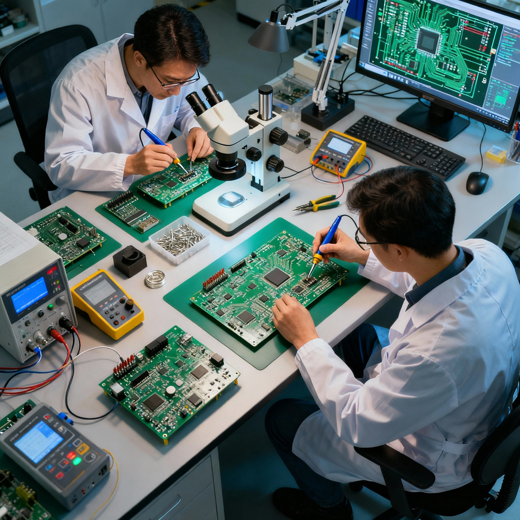
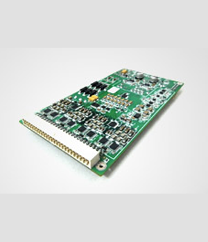
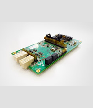
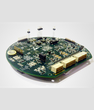
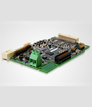
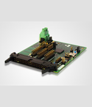
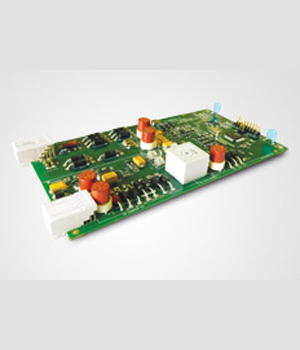
Printed Circuit boards are physical and electrical scaffolds that hold the electronics together and designing them requires a lot finesse and ingenuity. Our team of experienced engineers work closely with customers to design reliable, cost effective and rugged circuit boards considering various points:
If the need arises, we work closely with reputable Printed Circuit Board fabrication houses to qualify designs for DFM. Our key differentiator is our rigorous, proprietary design and review process that ensures reliable result in minimal time.
If your technology is draining resources rather than optimizing them, we can get you back on track. A professionally managed services provider can give you the decisive edge to:
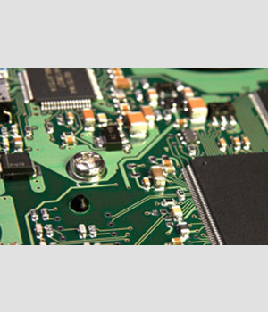
PCB testing services are offered optionally in conjunction with layout design.
We use a combination of automatic and semi-automatic tools or hand placement as per need dictated by PCB design and density, component types and sizes to create clean-cut protos suitable for immediate testing. The same engineers who may have created PCB layout design work side-by-side with prototyping technicians as an advantage. The following points are considered:
We would really like to hear from you and answer any questions. Please email us at info1@ascenten.net
or call us on
India Mobile: +91-89800 00973
India Landline: +91-79-2646 4646
Home | Careers | Ethics | Privacy Policy | Terms Of Use | Code Of Conduct
