Home > FPGA Bridge
Admin | Posted on 20/06/12
When we talk of precision instrumentation, we are looking at a system that can manage highly complex math-intensive tasks, since the data collected from physical sensors need a complex degree of calculations to be measured. Although a DSP is well suited for extremely complex math-intensive tasks, it cannot process high sampling rate applications due to its serial architecture.
ASIC does meet all the constraints of digital signal processing, however, it lacks flexibility and requires long design cycles. FPGA overcomes the disadvantages of ASIC and DSP with flexibility, time-to-market, risk-mitigation and lower system costs. FPGA is ideal for implementing data formatting, timing, and specialized glue logic needed to connect real-time peripherals like modems, A/D converters and digital receivers to programmable processors.
Now what exactly is an FPGA Bridge and why is it an important design aid? To put this case in point, let me elaborate a design challenge I recently encountered while trying to interface an ADS5474EVM ADC Board and a TMS320C6455 DSK DSP Kit. The DSP required data from an analog sensor for processing. It activated the sensor by providing a capture pulse to it. The sensed analog data was digitized by ADS5474EVM ADC Board at 400 MSPS rate. TMS320C6455 DSK DSP Kit which required this digitized data from ADC for further processing was not able to sample the incoming data at such a high rate. So a need arose to implement a bridge circuit, that could sample data at 400 MSPS and store data equivalent to 20 ms (approx. 8 million samples) from the captured signal. The FPGA Bridge was designed to provide seamless interface between ADS5474EVM ADC Board and TMS320C6455 DSK DSP Kit. The FPGA bridge was a proof of concept that data at 400MSPS from ADC can be sampled at 200 MHz DDR rate by a Spartan 3a DSP (maximum operating frequency is 250 MHz), suitably stored and provided to DSP processor for further processing.
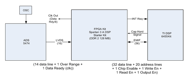
The above block diagram shows the top level interface diagram from ADS-5474 kit to FPGA Kit to TI-DSP 6455.
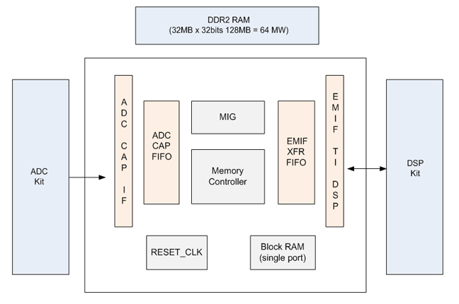
RESET_CLK modules generate synchronous reset and skew free clocks to the respective modules.
ADC_CAP_IF: LVDS data capture module used to capture ADC sample and transfer 2 samples to Asynchronous FIFO.
ADC_CAP_FIFO: Asynchronous FIFO with Dual Port BLOCK RAM, the block RAM size is 8K x 32 bits at write side and 4K x 64 bits at read side.
MEMORY_CTRL: Memory Controller Module transfers data from ADC_CAP_FIFO to MIG DDR2 controller and also performs data transfer from MIG DDR2 controller to EMIF_FIFO.
MIG DDR2 controller transfers data to and from DDR2 memory based on the command-data from Memory Controller.
EMIF_FIFO: Asynchronous FIFO with Dual Port Block RAM, the block RAM size is 2K x 64 bits at write side and 4K x 32 bits at read side.
EMIF_IF: 32-bit EMIF Interface with Interrupt to TI-DSP and controlling the entire data transfer by generating appropriate control signals to and reception of status signals from ADC capture and Memory Controller.
| Module Name | Clock Domain | Input Data Width | Output Data Width |
|---|---|---|---|
| ADC CAPTURE Module | In: adc_cap_clkOut: adc_cap_clk | 14 Bits data + OVR from ADC IC | 32 Bits (2 Samples of ADC Inputs) |
| ADC_CAP_FIFO | In: adc_cap_clkOut: core_clk | 32 Bits (2 Samples of ADC Input) | 64 Bits to Memory Controller |
| Memory Controller | In: core_clkOut: core_clk | 64 Bits Data from ADC_CAP FIFO | MIG controller (64 Bits) |
| Memory Controller | In: core_clkOut: core_clk | 64 Bits Data from MIG controller | 64 Bits data to EMIF FIFO |
| MIG controller (DDR2 Controller Core) | In: core_clkOut: core_clk | 64 Bits data to/from Memory Controller | 32 bits DDR data to DDR2 Memory |
| EMIF FIFO | In: core_clkOut: core_clk | 64 bits data from Memory Controller | 32 bits data to EMIF Controller |
| EMIF Interface | In: core_clkOut: core_clk | 32 Bit Data from EMIF FIFO | 32 Bit Data to TI-DSP using EMIF Protocol |
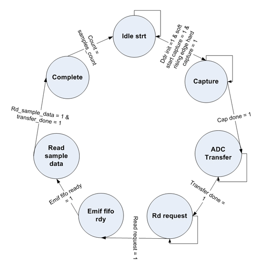
Idle State:
Whenever FPGA is reset, powered up, or completes a data transfer, the FSM is in this state. The FSM remains here until:
- DDR2 is initialized
- Soft Start capture is set to 1 in the control register
- Rising edge of the hard capture is detected
When all three conditions are satisfied, the FSM moves to the Capture state and generates a capture enable signal for the ADC Capture module to start capturing samples. In this state, the status register is updated on every clock.
Capture State:
FSM remains in the Capture state until it receives a capture done signal indicating the required number of samples have been captured. If capture done was due to a forced stop, an interrupt is generated to the DSP. Capture enable is set to zero, and FSM jumps to the ADC Transfer state. Status register is updated on every clock.
ADC Transfer State:
FSM remains in this state until it receives a transfer done signal, indicating that the required samples have been transferred to DDR2 memory. An interrupt is generated to DSP if the corresponding bit in the Interrupt Mask Register is set. FSM then jumps to the Read Request state. Status register is updated on every clock.
Read Request State:
FSM waits for DSP to write the Read Request bit in the control register, indicating that DSP is ready to fetch data. When the bit is set to 1, FSM jumps to the FIFO Ready state and generates the DDR EMIF Transfer Enable signal to the Memory module to start dumping data from DDR2 memory to EMIF FIFO. The actual samples count register is written in this state.
FIFO Ready State:
FSM waits until EMIF FIFO has 64 samples of data. It updates the status register to indicate to DSP that data is ready in the FIFO and generates an interrupt if the corresponding bit in the Interrupt Mask Register is set. Status register is updated on every clock.
Read Sample Data State:
FSM waits for DSP to write the Read Sample Data bit in the control register, indicating DSP has acknowledged FIFO Ready and FSM should continue dumping data from DDR2 memory to EMIF FIFO. FSM remains in this state until it receives the DDR EMIF Transfer Done signal, indicating all samples stored in DDR2 memory have been transferred to EMIF FIFO. Status register is updated on every clock.
Complete State:
FSM waits until all the samples entered in the sample count register have been fetched, then jumps to Idle state. FSM generates an interrupt indicating process completion if the corresponding bit in the Interrupt Mask Register is set. Status register is updated on every clock.
FPGA, acting as a bridge, is able to sample data from ADC at 400 MSPS while simultaneously transferring and storing up to 16 million samples in DDR2 memory. This allows the DSP to process large chunks of data without loss, by fetching it from DDR2 memory through the FPGA EMIF interface.
We would really like to hear from you and answer any questions. Please email us at info1@ascenten.net
or call us on
India Mobile: +91-89800 00973
India Landline: +91-79-2646 4646
Home | Careers | Ethics | Privacy Policy | Terms Of Use | Code Of Conduct
